

This is the state-of-the-art technology developed by OSAKA SMEs. At the MOBIO Tech Hall, you can discover amazing technologies!
FUJI SEIMITSU KOGYO CO., LTD.:https://www.m-osaka.com/en/exhibitors/044/
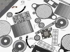
Welcome to the world of micro magic by FUJI SEIMITSU. When customers need a 10 times higher processing accuracy and ultra-fine processing than photo etching, with a plate thickness of 0.005 to 0.035 mm and a minimum hole size of 20μ, FUJI is capable to offer its optimal electroforming process.
FUJI has developed exclusive masking process with photoresist (photosensitive corrosion resistant film) on the substrate, transferring the pattern with the photomask, and electroforming (forming nickel) on the exposed portion of the substrate to obtain the desired shape.
Naturally, it has no burr or distortion and is used in various applications such as optics, precision and electronic equipment.
Study FUJI SEIMITSU's micro magic displayed at the 2nd floor of the MOBIO Tech Hall.